The advancement of silicon electronic technology is slowing down as the field becomes more mature and the technology scaling approaches the quantum limit. However, there are many current and emerging impactful open areas of research such as quantum engineering assisted electronics, non-planar transistor based electronic systems, low power mm-wave and THz signal generation, processing, and imaging, AI assisted analog and RF systems, as well as analog and RF assisted AI systems. At the same time, the field of silicon electronics is rapidly becoming interdisciplinary to advance further.

ELECTRONIC PHOTONIC CO-DESIGN
For a given silicon electronic technology, the performance of the active and passive devices is mainly limited by the parasitic components (such as undesired capacitance and resistance) and the substrate loss. The active device level limitations make the signal generation and processing rather challenging at sub-mm-wave and THz regimes. Also, parasitic components of the active devices together with the limited quality factor of passive components make the design of low phase noise oscillators and efficient power amplifiers rather challenging. Additionally, the loss and limited bandwidth in the high-frequency electrical interconnects increase the power consumption of chip-to-chip or board-to-board data links significantly.
Quantum engineering and innovative new devices (such as non-planar active and passive devices) may overcome some of the active and passive device level challenges and are important and promising open areas of research. Moreover, the performance of some of the RF, mm-wave, and sub-mm-wave systems that are designed in silicon based technologies may be improved through the concept of electronic-photonic co-design. The low loss of the optical medium (such as waveguides), as well as the high bandwidth available in optical frequencies can be employed to improve the performance of an existing electronic system. Low-loss optical delays and high quality factor resonators available in the photonic integrated circuits can be used to perform optically assisted electrical signal processing. Due to the small size of these photonic resonators, the optically assisted electrical signal processing may be performed in a smaller area compared to an equivalent all-electrical system. Similarly, use of sophisticated analog, RF, mm-wave, and sub-mm-wave architectures in addition to near-zero incremental cost of transistors in high node technologies can improve the performance of photonic systems. Examples are RF assisted phase noise reduction of semiconductor lasers and electronically controlled laser phased arrays. In the concept of electronic-photonic co-design, combining the advantages of devices, circuits, and architectures in both electronic and photonic domains can profoundly impact both fields resulting in advances in several areas such as communications, computation, signal processing, imaging, sensing, and bio-technology. Under the ONR YIP program, we have demonstrated an integrated end-to-end photonic deep neural network (PDNN) chip that can perform image classification at a rate of nearly 1.8 billion-frames-per-second through direct processing of the optical waves impinging on the on-chip pixel array as they propagate through layers of neurons. Under the DARPA photonic assisted integrated ultra-low phase noise clock (Pi-UPNC), we have implemented the first integrated nanophotonic phase noise filter, which can be placed after a low-cost laser to significantly suppress its phase noise independent of the light source. More than 4 orders-of-magnitude laser linewidth reduction using the hybrid integrated photonic phase noise filter has been achieved. As an example of photonic assisted electronics, we have implemented a photonic-assisted mm-wave phased array transmitters for direct fiber to mm-wave links, where an electronic-photonic transmitter chip utilizes optical heterodyning within an electronically controlled photonic network for mm-wave generation, beamforming, and steering. As another example of photonic assisted electronics, we have demonstrated the first single-chip nanophotonic microwave near-field imager, where the chip first up-converts the impinging microwave signals (pulses) to the optical domain and optically delays and processes the signal to form the near-field image of the target object. The implemented imager utilizes photonic delay lines with about 44 times smaller chip area compared to the equivalent state-of-the-art electrical delay lines and achieve more than 16 times lower propagation loss. Under the DARPA DODOS program, we have developed a highly stable optical synthesizer with sub-Hz level resolution across 5THz range. Under this program, we have also demonstrated the first fully integrated Pound Drever Hall (PDH) laser stabilization system in CMOS. Under DARPA MOABB program, we implemented 2D optical phased arrays with a record element pitch. Under DARPA QuICC program we are working toward implementation of electronic-photonic Ising machines. Under DARPA WARP program we are working on implementation of an integrated photonic-acoustic system for self-interference cancellation in full-duplex transceivers.


NEXT-GENERATION OPTICAL TRANSCEIVERS
With the rapid growth of social media, AI platforms, video streaming, and cloud services, we are witnessing an ever-increasing capacity demand from the inter-rack links to the global IP network. This requires the next generation transceivers to be low cost, highly scalable, and energy efficient. All-silicon transceivers have the potential to be mass-produced at low costs. By leveraging the CMOS-compatible silicon photonics and the advanced electronic processes, we are developing optical transceivers for next generation networks. The co-design of the photonic devices and mm-wave electronic circuitry enables realization of high-speed low-power and low-cost monolithically integrated transceivers. Under DARPA PIPES program, we have been working on implementation of monolithic electronic-photonic massive links that provides extreme scalability for data communication by integration of a frequency comb into silicon-photonics-on-CMOS platform aiming for 100 Tb/s data-rates and beyond. Record energy efficiency and areal bandwidth density for integrated WDM systems have been achieved.

BIO-ELECTRONICS AND BIO-PHOTONICS
Brain-machine-interface (BMI) plays a significant role in understanding the brain and treating diseases such as epilepsy, Parkinson’s, Alzheimer’s, etc. Next-generation BMI requires an ultra-low power chip to precisely process neural signals and decrease the wireless data bandwidth thus enabling high recording channel-count while preventing tissue damage caused by heat dissipation.
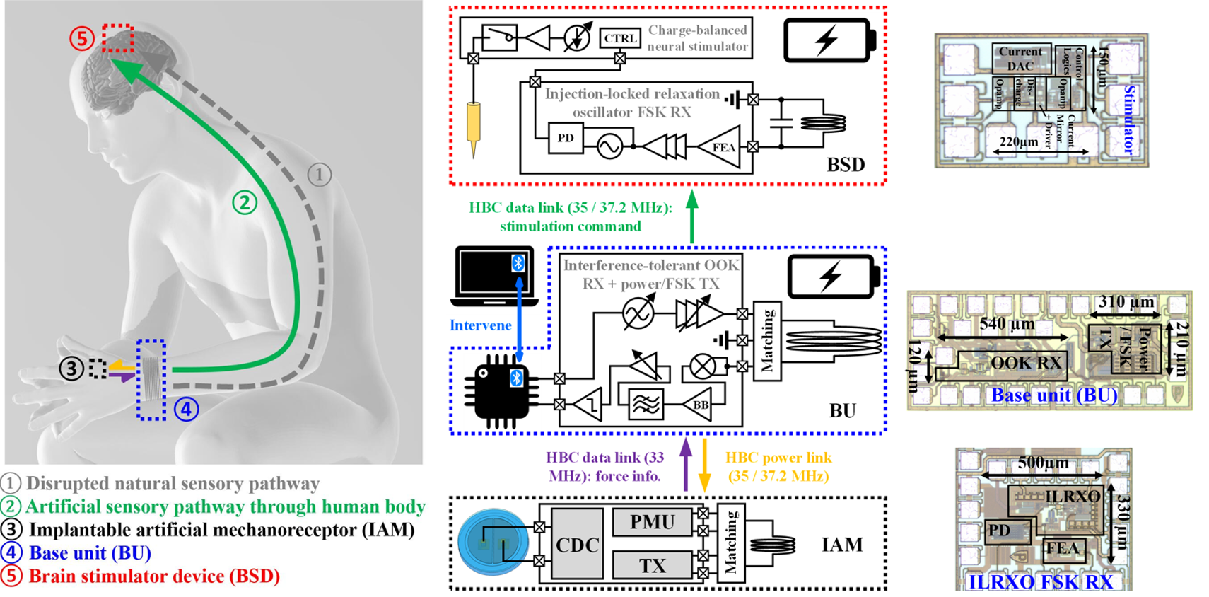
Wireless Somatosensory Feedback System Using Human Body Communication – we have implemented the first integrated somatosensory feedback system based on human body communication. The multi-chip system is composed of a wrist device, a brain stimulator device, and an artificial mechanoreceptor, and is designed to restore the sense of touch to a paralyzed hand through tactile sensing and neural stimulation. By utilizing the human body communication technique, multiple highly efficient wireless links are realized through the low loss body channel.
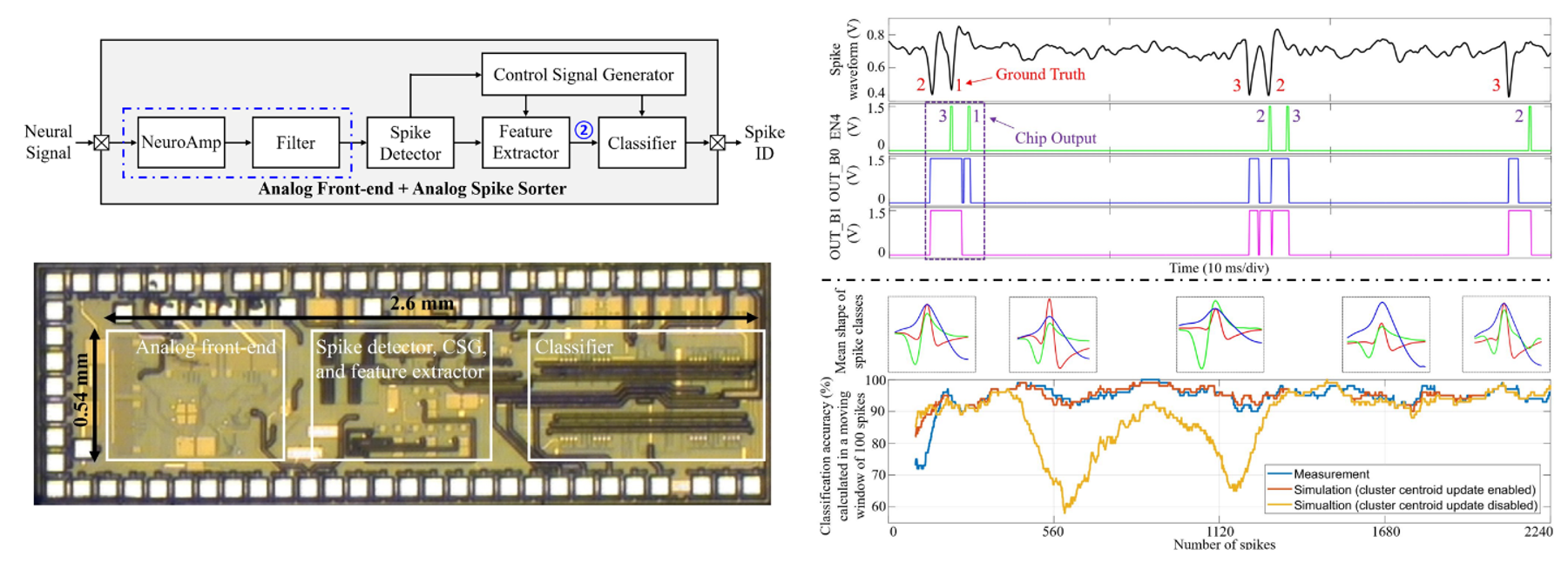
Low power machine learning for on-chip neural signal processing – a specific processing task performed on extra-cellularly recorded neural signal is spike sorting, which distinguishes the firing activities of multiple neurons based on the difference between their electrical waveforms. By integrating all of the essential blocks on a CMOS chip, including signal conditioning, feature extraction and classification, we are working toward a self-contained spike sorter that bridges between the raw extra-cellular neural signals and the single neuron activities. Featuring a novel classification algorithm and its analog implementation, the spike sorter chip is expected to achieve high accuracy at an ultra-low power consumption.
Rapid in-flow cell analysis – we are developing on-chip sensor arrays for rapid in-flow analysis of cells and nanoscale biological particles. The high-speed processing capabilities of integrated electronic and photonic circuits allow us to parallelize operation of the sensing array elements. This is critical in breaking the tradeoff between sensitivity and throughput hence improving the effectiveness of these biosensors as tools for fundamental biological studies and clinical monitoring of disease. We are exploring heterogeneous integration of these circuits with microfluidics and 2D material sensors to further enhance sensitivity and speed.
ELECTRONICS for QUANTUM SPIN CONTROL
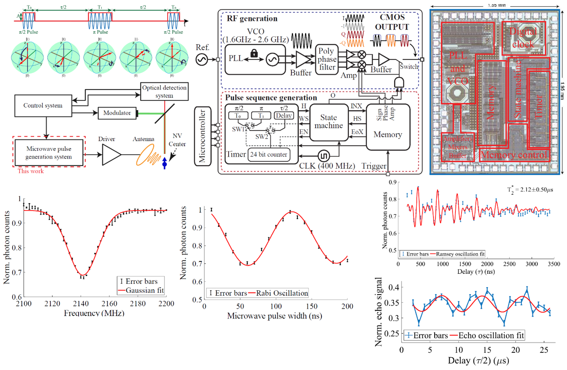
Under NSF RAISE-EQuIP we have implemented a low-power CMOS chip that processes and generates the necessary RF, analog, and digital signals for spin resonance control and real-time adaptive feedback control in a quantum memory.